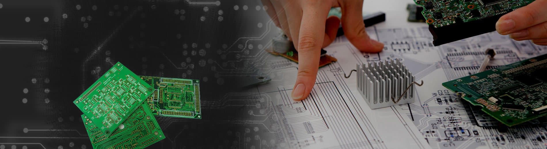
QUOTE REQUESTFree, Fast, & Secure

Custom PCB Manufacturing

Background

Custom PCB Manufacturing, Printing, PCB Fabrication

QUALITY MANUFACTURING AND FABRICATION

Why Buy From Avanti Circuits?

  • Quality
  • Speed
  • Experience
  • Cost
  • Outstanding Customer Service

We are a U.S.-based, custom printed circuit board manufacturer with full, in-house manufacturing capabilities. We have been in business since 1982- specializing in quick turn, high quality custom PCB fabrication. For three decades Avanti Circuits has been a leading pcb manufacturer in the United States specializing in Quickturn Printed Circuit Boards.

Our mission is to provide you with the best service and fabrication in the industry. We offer custom quotes, superior customer service, and on time deliveries. We stand behind our products 100% and take pride in a close and cooperative partnership with our customers.
  • Fast online quotes
  • Quick turn delivery. Same day turn available on two layer PCB, 24 hour turn available on multilayer PCB.
  • In inventory materials include FR4, Rogers, Polyimide and more.
  • Available finishes include HASL, Lead free HASL, Nickel/Gold, soft bondable gold, ENIG, ENEPIG, immersion Tin, immersion Silver, Carbon Ink,
  • and more
  • Copper weight 0.25 oz to 4 oz.
  • Prototype to full production PCB.
  • Made in the USA for over 30 years.
Prototype PCB Board

A proud Avanti employee shows a PCB midway through the manufacturing process.

At Avanti Circuits, our custom PCB manufacturers know their way around a circuit board. We employ only the most driven and knowledgeable staff for printed circuit board manufacturing to ensure that you get the quality products you need every time. Just let our friendly customer service representatives know what you’re looking for and we’ll point you in the direction of the custom PCB manufacturing services you need to complete your latest project. The best part? Avanti Circuits are guaranteed. All our products are put through a thorough quality control check before they leave our facility. We’re confident in our work, and when you work with us, you’ll find out why!

When we say Avanti Circuits offers custom products, we mean it. We have a fantastic reputation in the PCB manufacturing industry for providing our customers with the parts they need, no matter how nuanced. Give us a call today at 1-888-595-8876 to discuss your specific multi-layer PCB or quick turn PCB manufacturing requests. You can also head over to the Contact Us page and request a quote by filling out our quick and easy email form. Quotes are 100 percent free. Whether you’re a private contractor or you have a business of your own, we’re happy to form a harmonious bond with you that will benefits both parties.

PCB Manufacturing Process

There is a lot that goes into manufacturing a PCB. Here is our brief tutorial on the printed circuit board manufacture process.

What does it take to build Printed Circuit Boards?

Introduction to Manufacturing

When it comes to electronics, printed circuit boards are used to mechanically support and electrically connect electronic components using conductive pathways, or traces, etched from copper sheets laminated onto a non-conductive substrate. Alternative names are printed wiring board or PWB or etched wiring board.

Printed circuit boards are rugged, inexpensive, and can be highly reliable. They require much more layout effort and higher initial cost than either wire-wrapped or point-to-point constructed circuits, but are much cheaper, faster, and consistent in high volume production.

The two major stages for manufacturing a printed circuit board are:
  • Printed Circuit Board Design
  • Printed Circuit Board Manufacturing (PCB Fabrication)
Printed Circuit Board Design

Usually an electronics or electrical engineer designs the circuit, and a layout specialist designs the Printed circuit board. The designer must obey numerous PCB layout guidelines to design a PCB that functions correctly, yet is inexpensive to manufacture.

The Circuit Design

The Circuit Diagram, also called the Schematic or Logic Diagram, maps out the electronics and connections in the most readily readable form. The designer needs to do background work while producing the Circuit diagram, researching specifications of components, interaction between components (especially timing and loading) physical packages, and arrangement of connector pinouts. The circuit will often start on paper and finish in Computer Aided Design (CAD) format. The finished circuit diagram, supported by notes if required, is the main reference document for the design.

PCB Manufacturing Techniques
Electronic Design Automation (EDA)

PCB designers often use electronic design automation to produce a layout. The EDA program stores design information, facilitates editing the design, and can also automate repetitive design tasks.

The first stage is converting the circuit schematic into a net list. The net list is conceptually a list of component pins and the circuit nodes, or nets that each pin connects to. Often the schematic capture EDA program, operated by a circuit design engineer, is responsible for netlist generation, and the netlist is imported into the PCB layout program.

The next step is to decide the position of each device. The easy way to do this is to specify a grid of lettered rows and numbered columns where the devices should go. The computer then assigns pin 1 of each device in the bill of materials to a grid location. Typically, the operator may assist the automated placement routine by specifying rooms, or specific regions of the circuit boards, where certain groups of components should be placed. For example, the parts associated with a power supply subcircuit might be assigned to a region near the power input connector. In other cases devices may be manually placed, either to optimize the electrical performance of the circuit, or to place components such as knobs, switches, and connectors as required by the mechanical design of the system.

The computer then explodes the device list into a complete pin list for the circuit board by using templates from a library of footprints associated with each type of device. Each footprint is a map of a device’s pins, usually with a recommended pad and drill hole layout for each device. The library allows the footprint to be drawn only once, and then shared by all devices of that type.

In some systems, high-current pads are identified in the device library, and the associated nets are flagged for attention by the PCB designer. High current runs require wider traces, and the designer or circuit design engineer usually decides the width.

The computer program then merges the netlist (sorted by pin name) with the pin list (sorted by pin name), transferring the physical coordinates of the pin list to the netlist. The netlist is then resorted, by net name.

Some systems can optimize the design by swapping the positions of parts and logic gates to reduce the length of copper runs. Some systems also automatically discover power pins in the devices, and generate runs or vias to the nearest power plane or conductor.

The programs then try to route each net in the signal-pin list, finding some sequence of connections in the available layers. Often layers are assigned to power and ground, with one layer to vertical, and another to horizontal wires. The power layers shield the circuits from noise.

The routing problem is equivalent to the traveling salesman problem, and is therefore NP complete, and therefore not amenable to a perfect solution. One practical routing algorithm is to pick the pin farthest from the center of the circuit boards, then use a greedy algorithm to select the next-nearest pin with the same signal name.

After automated routing, usually there is a list of nets that must be manually routed.

Once routed, the system may have a series of strategy subroutines to reduce the production cost of the PCB. For example, one routine might remove unneeded vias (each via is a drill hole, and costs money to make). Another might round edges of conductor runs, and widen or move runs apart to maintain safe spacing. Another strategy might adjust large copper areas so that they form nets, or large blank areas may get unconnected “checks” of copper. The nets and checks reduce pollution by extending the life of the etching bath, and speed production by evening-out the copper concentration in the etching bath.

Some systems provide design rule checking to validate the design for electrical connectivity and clearance, rules for circuit board manufacture, assembly and test, heat flow and other errors.

The silk-screen, solder mask, and solder paste stencil(s) are often designed as auxiliary layers.

Finally, the copper layers are then converted to Gerber files, a format of numerical control file for a photoplotter. Historically, an additional aperture file was required to link each numerically designated aperture referred to in the Gerber file with an actual shape to be plotted. Newer Gerber files embed the aperture information in the Gerber file itself. The hole locations are encoded in drill files. The drill files may be sorted to minimize drill-head movement time, and bit changes.

Physical composition

Most PCB are composed of between one and sixteen (or even more) conductive layers separated and supported by layers of insulating material (substrates) laminated (glued) together. Layers may be connected together through drilled holes called vias. Either the holes are electroplated or small rivets are inserted. High-density PC may have blind vias, which are visible only on one surface, or buried vias, which are visible on neither.

Substrates

Low-end consumer grade PCB substrates frequently are made of paper impregnated with phenolic resin, sometimes branded “Pertinax”. They carry designations such as XXXP, XXXPC, and FR-2. The material is inexpensive, easy to machine by drilling, shearing and cold punching, and causes less tool wear than glass fiber reinforced substrates. The letters “FR” in the designation indicate Flame Resistance.

High-end consumer and industrial circuit board substrates are typically made of a material designated FR-4. This consists of a woven fiberglass mat impregnated with a flame resistant epoxy resin. It can be drilled, punched and sheared, but due to its abrasive glass content requires tools made of tungsten carbide for high volume production. Due to the fiberglass reinforcement, it exhibits about five times higher flexural strength and resistance to cracking than paper-phenolic types, albeit at higher cost.

PCB for high power radio frequency (RF) work use plastics with low dielectric constant (permittivity) and dissipation factor, such as Rogers® 4000, Rogers® Duroid, DuPont® Teflon® (types GT and GX), polyimide, polystyrene and cross-linked polystyrene. They typically have poorer mechanical properties, but this is considered an acceptable engineering tradeoff in view of their superior electrical performance.

PCB designed for use in vacuum or in zero gravity, as in spacecraft, being unable to rely on convection cooling, often have thick copper or aluminum cores to dissipate heat from electrical components.

Not all circuit boards use rigid core materials. Some are designed to be very or slightly flexible, using DuPont’s® Kapton® polyimide film, and others. This class of boards, sometimes called flex circuits, or rigid-flex circuits, respectively, are difficult to create but have many applications. Sometimes they are flexible to save space (PCBs inside cameras and hearing aids are almost always made of flex circuits so they can be folded up to fit into the limited available space). Sometimes, the flexible part of the circuit board is actually being used as a cable or moving connection to another board or device. One example of the latter application is the cable connected to the carriage in an inkjet printer. Power electronic applications require low-thermal resist-substrates, with thick copper track to carry high currents. The main technologies are ceramic-based substrates (Direct Bonded Copper) and metal-based substrates (Insulated Metal Substrate).

Manufacturing Technique(s)

Patterning/Imaging

The vast majority of “printed circuit boards” are made by adhering a layer of copper over the entire substrate, sometimes on both sides, (creating a “blank PCB”) then removing unwanted copper after applying a temporary mask (e.g. by etching in ferric chloride), leaving only the desired copper traces. A few PCBs are made by adding traces to the bare substrate usually by a complex process of multiple electroplating.

There are three common methods used for the production of printed circuit boards:
  • Silk screen printing uses etch-resistant inks to protect the copper foil. Subsequent etching removes the unwanted copper. Alternatively, the ink may be conductive, printed on a blank (non-conductive) board. The latter technique is also used in the manufacture of hybrid circuits.
  • Photoengraving uses a photomask and chemical etching to remove the copper foil from the substrate. The photomask is usually prepared with a photoplotter from data produced by a technician using computer-aided PCB design software. Laser-printed transparencies are sometimes employed for low-resolution photo plots.
  • PCB Milling uses a 2 or 3 axis mechanical milling system to mill away the copper foil from the substrate. A PCB milling machine (referred to as a ‘PCB Prototyper’) operates in a similar way to a plotter, receiving commands from the host software that control the position of the milling head in the x, y, and (if relevant) z axis. Data to drive the Prototyper is extracted from files generated in PCB design software and stored in HPGL or Gerber file format.
Lamination

Some PCBs have trace layers inside the PCB and are called multi-layer PCBs. These are formed by bonding together (using high pressure in a press) separately etched thin boards.

Drilling

Holes, or vias, through a PCB are typically drilled with tiny drill bits made of solid tungsten carbide. The drilling is performed by automated drilling machines with placement controlled by a drill tape or drill file. These computer-generated files are also called numerically controlled drill (NCD) files or “Excellon files”. The drill file describes the location and size of each drilled hole.

When very small vias are required, drilling with mechanical bits is costly because of high rates of wear and breakage. In this case, the vias may be evaporated by lasers. Laser-drilled vias typically have an inferior surface finish inside the hole. These holes are called micro vias.

It is also possible with controlled-depth drilling, laser drilling, or by pre-drilling the individual sheets of the PCB before lamination, to produce holes that connect only some of the copper layers, rather than passing through the entire circuit board. These holes are called blind vias when they connect an internal copper layer to an outer layer, or buried vias when they connect two or more internal copper layers.

The walls of the holes, for circuit boards with 2 or more layers, are plated with copper to form plated-through holes that electrically connect the conducting layers of the PCB.

Custom Printed Circuit Boards Machine
Solder plating and solder resist

The pads and lands to which components will be mounted are typically plated, because the bare copper is not readily solderable. Traditionally, any exposed copper was plated with solder. This Printed Circuit Board Press

Press used in manufacturing custom printed circuit boards.

solder was traditionally a tin-lead alloy, however new solder compounds are now used to achieve compliance with the RoHS directive in the EU, which restricts the use of lead. Edge connectors, made on the sides of some circuit boards, are often gold plated. Gold plating is also sometimes applied on the whole boards.

Areas that should not be soldered to may be covered with a polymer solder resist coating. The solder resist prevents short circuits between nearby component leads.

Silk screen

Line art and text may be printed onto the outer surfaces of a PCB by silk screening. When space permits the silk screen text can indicate component designators, switch setting requirements, test points, and other features helpful in assembling, testing, and servicing circuit boards. In one sided PCBs, silk screen is also known as the ‘red print’.

Populating

In through-hole construction, component leads may be inserted in holes and electrically and mechanically fixed to circuit board with a molten metal solder. In surface-mount construction, the components are simply soldered to pads or lands on the outer surfaces of the PCB. Often through-hole and surface-mount construction must be combined in a single PCB because some required components are available only in surface-mount packages, while others are available only in through-hole packages.

Test and validation

Unpopulated boards may be subjected to a bare-board test where each circuit connection as defined in a netlist is verified as correct on the finished board. For high-volume production, a Bed of nails tester or fixture is used to make contact with copper lands or holes on one or both sides of the board to facilitate testing. A computer will instruct the electrical test unit to send a small amount of current through each contact point on the bed-of-nails as required, and verify that such current can be seen on the other appropriate contact points. For small- or medium-volume circuit boards, flying-probe testers use moving test heads to make contact with the copper lands or holes to verify the electrical connectivity of the board under test.

Protection and packaging

PCBs intended for extreme environments often have a conformal coat, which is applied by dipping or spraying after the components have been soldered. The coat prevents corrosion and leakage currents or shorting due to condensation. The earliest conformal coats were wax. Modern conformal coats are usually dips of dilute solutions of silicone rubber, polyurethane, acrylic, or epoxy. Some are engineering plastics sputtered onto the PCB in a vacuum chamber. Mass-production PCBs have small pads for automated test equipment to make temporary connections. Sometimes the pads must be isolated with resistors.

QUOTE REQUESTFree, Fast & Secure

PCB Manufacturing Departments

Engineering and Cam Area

  • 4 Apollo CAM Workstations
  • 3 Genesis CAM Workstations
  • 1 Checkmate II Drill Programmer
  • 1 Micro modifier
  • 1 EIE PHOTO PLOTTER
  • 1 Kodamatic 710 Film Processor
  • 1 Cimnet Integrated
  • MFG Software System
  • FR-4 (Tg =135′, 145′, 170′ C)
  • N4000-13 (modified epoxy)
  • Rogers Duroids & Teflons
  • Getek, BT Epoxy, Polyimides
ML Lamination Area
  • 1 Custom Black Oxide Line
  • 1 Wabash 4 Opening Vacuum Press
  • 1 Wabash 2 Opening Press
  • 2 PHI 2 Opening Presses
  • 1 Circuit Machine Model 7500 Saw
  • 1 Multiline Pinning System
  • Min Board Thickness: 0.005”
  • Max Board Thickness: 0.250”
  • Min Core Thickness: 2.5 mils
  • Min Prepreg Thickness: 2.0 mils
  • Thickness Tolerance: +/- 10%
Printed Board Drill Area
  • 1 Tennsmith 48” Power Shear
  • 2 Barnaby Stackmaster
  • 1 Excellon MK-6 Drill
  • 1 Excellon MK-5 Drill
  • 2 Excellon XL-5 Drill
  • 1 Chemcut Model 547 Deburr System
  • Size: PTH +/- 3 mils, NPTH +/- 2 mils
  • Specific Tooling Holes: +/- 1 mil
PCB Imaging Area
  • 1 Somaca Scrubber
  • 3 Dry Film Laminators
  • 2 Colight Exposure units
  • 1 ORC 5 KW Exposure Unit
  • 1 Multiline Thin Core Punch
  • 1 VCM Vertical Developer
  • Layer to Layer + – 3 mils
  • Front to Back: +/- 2 mils
  • Soldermask: +/- 2 mils
  • Hole to Pad: +/- 5 mils (I/L tangency)
  • Hole to Pad: +/- 5 mils (O/L tangency)
PCB Plating
  • 1 Eidschun Shadow Line
  • 1 Custom Copper Plating Line
  • 1 Marseco Etcher
  • 1 Custom Dry Film Stripping Line
  • 1 Custom Tin Lead Stripping Line
Soldermask and Legend
  • 3 Precision Screening Tables
  • 1 Gyrex LPI Soldermask Sprayer
  • 1 DP-10 Soldermask
  • Screening Unit
  • 1 Soldermask Exposure Unit
  • 1 Chemcut Model 547 Scrubber
  • 3 Soldermask Curing Ovens
  • 2 VCM Vertical Developer
  • Per IPC-SM-840
  • LPI Types: Probimer 77 & Taiyo PSR4000
  • Wet Types: Dexter SR-1000 & SR-1020
  • Solder Mask Colors: green, Blue, Red, Clear, Black & White
  • Legend Colors: White, Black & Yellow
PCB Surface Finish
  • 1 Hot Oil Reflow Line
  • 1 Hot Air Leveling Line
  • 1 Deep Gold Panel Planting Plating Line
  • 1 Electroless Ni / Au Immersion Line
  • 1 Immersion Tin Line
  • SMOBC (soldermask over bare copper)
  • HASL (hot air solder leveling)
  • Fused Tin/ Lead Plating
  • Electroless Nickel / Immersion Gold
  • Electrolytic Nickel / Gold
  • Immersion Tin (Omikron)
  • Carbon Ink: 20 OHMS
PCB Fabrication Area
  • 3XL-3 Driller Pouters
  • 3 Barnaby Scoring Machines
  • 1 Acuscore CNC Scoring Machine
  • 1 Bevel master
  • 1 Marseco Final Clean Machine
  • Routing: Individual or Panelized Array
  • Scoring: Profiles & Route/ Score Combinations
  • Countersinks, Counterbores, Beveling & Edge Mining
  • Board Edge & Slots: Plated & Non-plated
Board Inspection And Test
  • 4 Inspection Work Stations
  • 1 Camtek 2V50P AOI
  • 2 Bausch & Lomb Stereo Microscopes
  • 1 LIXI X-ray Unit
  • 1 Beta Back Scatter Measurement Unit
  • 1 Comac Board Dryer
  • 3 Mania Flying Probe Testers
  • 1 Trace 924 Single Access Tester
  • 1 Everett Charles 9090 Dual Access Tester
  • Net List Testing per IPC-356D
  • Test Voltage: 100-250-volts
  • Continuity Resistance: 10-20 ohms
  • Isolation Resistance: 2-30 megaohms
  • Minimum SMT Pitch: 0.5 mm
Analysis Laboratory
  • 1 Complete Wet Analysis Laboratory
  • 1 Complete Micro Section Laboratory
  • 1 Perkins-Elmer AA Spectrophotometer
  • 1 Versamet
  • 2 1000X Microscope
PCB Manufacturing Support Area
  • 1 Memtek Water Management System
  • 1 Simpson Sludge Filter Press
  • 1 Sulliar 50 HP Air Compressor
  • 1 Worthington 30 HP Air Compressor
  • 1 LeRoi 40 HP Air Compressor
  • 1 Ingersoll-Rand 75 HP Air Compressor
  • 1 Trane 15 Ton Air Chiller
  • 1 RSD 15 Ton Air Cooling Tower
  • 2 Spencer 15 HP Vacuum Systems
PCB Board Types
  • Type II Single & Double Sided
  • Type III Multilayer through 24 layers Blind & Buried Vias
  • Plugged Vias (Conductive Ink)
  • Minimum Finished Via Size: ): 0.006”
  • Maximum Hole Aspect Ratio: 12:1
  • Minimum Line Width: 0.004”
  • Minimum Spacing: 0.004”
  • Edge to Edge +/- 5 mils
  • Tooling Holes to Edge +/- 4 mils