An Overview on Printed Circuit Boards
Printed circuit boards are known for being a very handy tool in the manufacturing industry. However, it’s not always clear what printed circuit boards are or how they’re made. This article aims to help you understand a little more about these very important products.
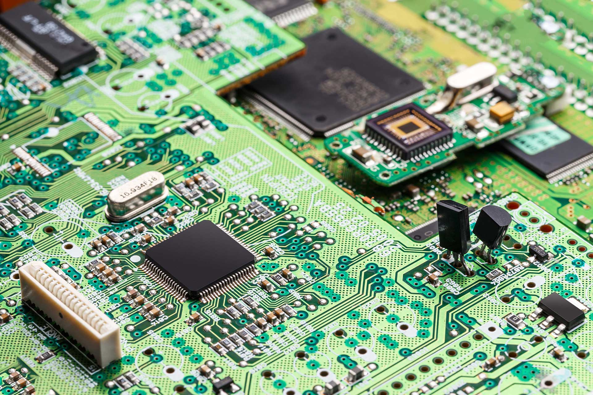
A Printed Circuit Board Assembly, PCB, connects electrical components via copper tracks and solder versus wire connections. Interconnectivity makes PCBs more durable and reliable than wire connectors. They’re also much less complex. When the first operational PCB was made in 1943 and then when printed circuit board manufacturers sprung up shortly thereafter, life, in many ways, was changed in a profound way. Put simply, the electronic gadgets, devices and appliances we enjoy today, from circuit boards in military equipment to your smart phone in large part are only possible because of the PCB and all its iterations.
Circuit board technology has continued to grow and evolve. Today, there are multiple types of circuit boards that make thousands of types of equipment functional. Here are the basic types of PCB and examples of where they are used.
What Exactly is a Printed Circuit Board?
Also known as a “Printed wiring card” or a “Printed wiring board”, printed circuit boards are a modern solution to larger circuit boards that took a lot of time to manufacture. The larger circuit boards needed to be wired from point to point and short circuits and failures were common. Thankfully, wire wrapping was invented and allowed for easier connection points to be created, and it was from this point where printed circuit boards were created.
A printed circuit board is made up of layers of materials that are laminated together. During the lamination process adhesives and tape are used so a single object is created.
What is a Printed Circuit Board Made of?
A PCB (Printed circuit board) is made up of substrate, copper, soldermask, and silkscreen.
- Substrate
The substrate (FR4) is a base material, typically fiberglass. The fiberglass gives the PCB its thickness and rigidity. Many PCBs are between 1.6 mm and 0.8 mm thick, depending on what they are being used for.
Inexpensive PCBs rend to be made of phenolics or epoxies which are not as durable as fiberglass but they are much cheaper. Inexpensive PCBs tend to let off a bad smell when they are being soldered, making them quite unpleasant to work with.
- Copper
The next layer on a PCB is copper. The copper is laminated to the board and might be attached to both sides of the substrate. The thickness of the copper can vary but they can help give the PCB a lot of power
- Soldermask
The soldermask is the layer that is located on the copper foil. This is the layer that gives the PCB its green color. It is placed onto the copper so it is insulated against contact with other metals, conductive parts, or solder.
- Silkscreen
Finally, a white layer is added to the PCB. This layer is added over the soldermask. Those silkscreen numbers and letters that you see on a printed circuit board allow it to be assembled easily. In addition to this, manufacturers often use these labels so people can understand the function of each LED or pin.
PCB Terminology
PCB’s are often made up of:
- Annular rings – This is a ring of copper around a plated hole.
- Drill hits – Places on a PCB where a hole needs to be.
- Fingers – Exposed metal pads on the edge of the board.
- Pads – Exposed metal that has a component soldered to it.
- Planes – A block of copper that is defined by borders.
- Plated through-hole – A hole on the PCB which has an annular ring attached.
- Slot – A hole in the PCB that isn’t round.
- Solder paste – Suspended solder.
- Solder jumper – A small amount of solder that connects two pins.
- Thermal – A trace that connects a pad and a plane.
- Trace – An unbroken path of copper.
- V-score – A cut through a board that allows it to be snapped.
- Via – A hole that allows a signal to pass from one layer to another.
Flex
Flex printed circuit board manufacturing (FPCB) create repeatable connections between electronic boards and that interconnectivity eliminates the need for discrete conductors for that function. This reduces the complexity in device assemblies and provides a more stable operating platform. Flex PCB designs can be very complex with very high signal trace densities and multilayer configurations.
Rigid Flex
Rigid Flex PCB manufacturers create FPCBs that can be permanently connected to a rigid PCB board. Designs of this nature are complex but allow for a reduction in complexity in final assembly. Flex ridged designs are ready upon receipt and allow for three-dimensional designs that can include connectivity between multiple rigid and flexible components.
Rigid
Rigid PCB design is used in situations where the circuit board cannot be bent. This allows for flex PCBs to be attached to a more stable base. For example, the section of flex PCB needing a surface mount will be reinforced with a rigid backing to eliminate flexing during use. Rigid PCBs are heavier than their flex counterparts, so if weight or size is an issue, this type of PCB is often the first type to be jettisoned in favor of a flex arrangement.
The electronic gadgets we have come to take for granted, from that old 8-track tape recorder to kitchen appliances to today’s smart devices all use Flex, Rigid or Rigid-Flex circuit boards. Many printed circuit board manufacturers use a combination of the three. Each configuration allows for electronic components to be consolidated, yet flexible in design, which gives options for design in both appearance and functionality.
Printed circuit boards are incredibly flexible tools that allow manufacturers to create small electrical appliances. More complicated than they look, PCB’s are now an essential tool in the modern manufacturing world.