Circuit Board Development Facts
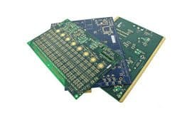
A printed circuit board, or PCB, is utilized to support and electrically connect electronic components using conductive pathways, tracks or signal traces etched from copper sheets laminated onto a non-conductive substrate.
Referred as printed wiring board (PWB) or etched wiring board, PCB populated with electronic components is called a printed circuit assembly (PCA). It is also known as a printed circuit board assembly (PCBA). Printed circuit boards are used in virtually all but the simplest commercially-produced electronic devices.
Avanti Circuits is a US-based PCB Manufacturer located in Phoenix, Arizona.
PCB Materials
Conducting layers are typically made of thin copper foil. Insulating layers dielectric are typically laminated together with epoxy resin prepreg. The board is typically coated with a solder mask that is green in color. Other colors that are normally available are blue and red. There are quite a few different dielectrics that can be chosen to provide different insulating values depending on the requirements of the circuit. Some of these dielectrics are polytetrafluoroethylene (Teflon), FR-4, FR-1, CEM-1 or CEM-3. Well known prepreg materials used in the PCB industry are FR-2 (Phenolic cotton paper), FR-3 (Cotton paper and epoxy), FR-4(Woven glass and epoxy), FR-5 (Woven glass and epoxy), FR-6 (Matte glass and polyester), G-10 (Woven glass and epoxy), CEM-1 (Cotton paper and epoxy), CEM-2 (Cotton paper and epoxy), CEM-3 (Woven glass and epoxy), CEM-4 (Woven glass and epoxy), CEM-5 (Woven glass and polyester). Thermal expansion is an important consideration especially with BGA and naked die technologies, and glass fiber offers the best dimensional stability.
AVANTI Circuits, utilizes the best materials for every project we undertake. Being a US-based manufacturer has its advantage versus overseas competition. Since we follow US Environmental Laws and Requirements, we use strict compliance in the use of materials and products. So we try to be Eco-friendly (Green) as much as we can be.
Design
Schematic capture or schematic entry is done through an EDA tool.
Card dimensions and template are decided based on required circuitry and case of the PCB.
Determine the fixed components and heat sinks if required.
Deciding stack layers of the PCB. 4 to 12 layers or more depending on design complexity. Ground plane and Power plane are decided. Signal planes where signals are routed are in top layer as well as internal layers.
Line impedance determination using dielectric layer thickness, routing copper thickness and trace-width. Trace separation also taken into account in case of differential signals. Microstrip, stripline or dual stripline can be used to route signals.
Placement of the components. Thermal considerations and geometry are taken into account. Vias and lands are marked.
Routing the signal trace. For optimal EMI performance high frequency signals are routed in internal layers between power or ground planes as power plane behaves as ground for AC. Gerber File generation for manufacturing.
Printed circuit assembly
After the printed circuit board (PCB) is completed, electronic components must be attached to form a functional printed circuit assembly, or PCA (sometimes called a “printed circuit board assembly” PCBA). In through-hole construction, component leads are inserted in holes. In surface-mount construction, the components are placed on pads or lands on the outer surfaces of the PCB. In both kinds of construction, component leads are electrically and mechanically fixed to the board with a molten metal solder.
There are a variety of soldering techniques used to attach components to a PCB. High volume production is usually done with machine placement and bulk wave soldering or reflow ovens, but skilled technicians are able to solder very tiny parts (for instance 0201 packages which are 0.02 in. by 0.01 in.) by hand under a microscope, using tweezers and a fine tip soldering iron for small volume prototypes. Some parts are impossible to solder by hand, such as ball grid array (BGA) packages.
Often, through-hole and surface-mount construction must be combined in a single assembly because some required components are available only in surface-mount packages, while others are available only in through-hole packages. Another reason to use both methods is that through-hole mounting can provide needed strength for components likely to endure physical stress, while components that are expected to go untouched will take up less space using surface-mount techniques.
After the board has been populated it may be tested in a variety of ways:
While the power is off, visual inspection, automated optical inspection. JEDEC guidelines for PCB component placement, soldering, and inspection are commonly used to maintain quality control in this stage of PCB manufacturing.
While the power is off, analog signature analysis, power-off testing.
While the power is on, in-circuit test, where physical measurements (i.e. voltage, frequency) can be done.
While the power is on, functional test, just checking if the PCB does what it had been designed for.
To facilitate these tests, PCBs may be designed with extra pads to make temporary connections. Sometimes these pads must be isolated with resistors. The in-circuit test may also exercise boundary scan test features of some components. In-circuit test systems may also be used to program nonvolatile memory components on the board.
In boundary scan testing, test circuits integrated into various ICs on the board form temporary connections between the PCB traces to test that the ICs are mounted correctly. Boundary scan testing requires that all the ICs to be tested use a standard test configuration procedure, the most common one being the Joint Test Action Group (JTAG) standard.
When boards fail the test, technicians may desolder and replace failed components, a task known as rework.
Conductor PCB plating and coating
PCBs are plated with solder, tin, or gold over nickel as a resist for etching away the unneeded underlying copper. After PCBs are etched and then rinsed with water, the solder mask is applied, and then any exposed copper is coated with solder, nickel/gold, or some other anti-corrosion coating.
Matte solder is usually fused to provide a better bonding surface or stripped to bare copper. Treatments, such as benzimidazolethiol, prevent surface oxidation of bare copper. The places to which components will be mounted are typically plated, because untreated bare copper oxidizes quickly, and therefore is not readily solderable.
Traditionally, any exposed copper was coated with solder by hot air solder levelling (HASL). The HASL finish prevents oxidation from the underlying copper, thereby guaranteeing a solderable surface. This solder was a tin-lead alloy, however new solder compounds are now used to achieve compliance with the RoHS directive in the EU and US, which restricts the use of lead. One of these lead-free compounds is SN100CL, made up of 99.3% tin, 0.7% copper, 0.05% nickel, and a nominal of 60ppm germanium.
It is important to use solder compatible with both the PCB and the parts used. An example is Ball Grid Array (BGA) using tin-lead solder balls for connections losing their balls on bare copper traces or using lead-free solder paste.
Other platings used are OSP (organic surface protectant), immersion silver (IAg), immersion tin, electroless nickel with immersion gold coating (ENIG), and directgold plating (over nickel). Edge connectors, placed along one edge of some boards, are often nickel plated then gold plated. Another coating consideration is rapid diffusion of coating metal into Tin solder. Tin forms intermetallics such as Cu5Sn6 and Ag3Cu that dissolve into the Tin liquidus or solidus(@50C), stripping surface coating and/or leaving voids.
Electrochemical migration (ECM) is the growth of conductive metal filaments on or in a printed circuit board (PCB) under the influence of a DC voltage bias. Silver, zinc, and aluminum are known to grow whiskers under the influence of an electric field. Silver also grows conducting surface paths in the presence of halide and other ions, making it a poor choice for electronics use. Tin will grow “whiskers” due to tension in the plated surface. Tin-Lead or Solder plating also grows whiskers, only reduced by the percentage Tin replaced. Reflow to melt solder or tin plate to relieve surface stress lowers whisker incidence. Another coating issue is tin pest, the transformation of tin to a powdery allotrope at low temperature.