How To Print Your Own Circuit Board
If you would like to print your own circuit board, you’ll be pleased to know that we can help you. Printing circuit boards ensure that a wide range of devices can work efficiently. No matter why you would like some circuit boards, we can help you.
Here at Avanti Circuits, we take pride in the work that we do. We have been working in this industry since 1982. When you choose to hire us to make your printed circuit boards you’re putting Americans to work.
Contact us today for a free estimate so you’re one step closer to having the PCBs you need. You can reach us at 602-866-7227. We’re here to help you with all of your PCB needs. Call us today.
What Is A PCB?
A printed circuit board is a board that works to connect a range of electronic components. In 1925, the very first electrical path was added to an insulated surface and patented. Since then, less complicated, much lighter designs have come into fruition. The designs are much easier to turn into usable printed circuit boards that we rely on every day.
Most people assume that printed circuit boards are made up of one layer of board. However, some boards have as many as 20 layers. Each of these layers interconnects and helps to reduce the overall size of the circuit board. When the circuit boards are smaller, the devices they sit in are smaller.
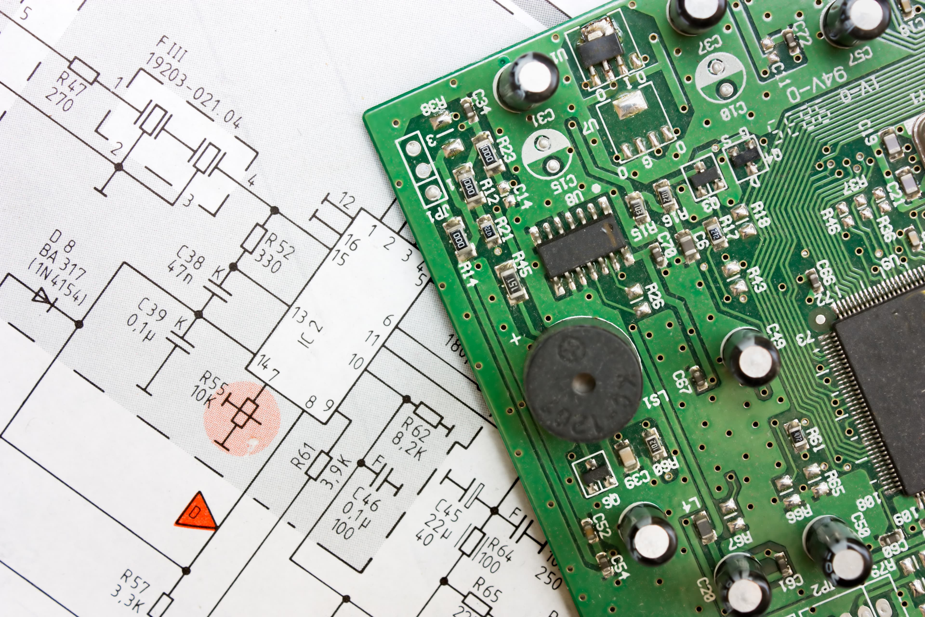
schematic diagram – design of electronic circuit and electronic board
Printing A Circuit Board
Printing your chosen circuit board can be quite a task. However, some people choose to print their own circuit boards at home. Many hobbyists find printing their own boards is a great way to build something special. However, if you need a circuit board for your products, you’ll need to make sure that they are professionally created.
The good news is that we can print your circuit board for you. We are a team of PCB professionals who have been in the industry since 1982. We are here to help you with all of your printed circuit board needs. No matter what you need the PCB for or how many you need, we can help you.
Whenever we print a customer’s circuit boards, we check them before we send them to the customer. We do this so that we can make sure the customer receives PCBs that work well, every time.
Create Your Circuit Design
When it comes to creating your PCB design, you need to understand a few things. You should ideally understand all of the electrical parameters associated with creating a design. YOu will need to know the following:
- Current maximums
- Signal types
- Voltages
- Capacitance limitations
- Shielding considerations
- Impedance characteristics
- Location and type of circuit connectors and components
- Detailed schematics and net wire listing
When you understand all of the above things, you can then begin to create your circuit board design.
Design Your Board Layout
– Designing the stackup
This stage of the design process involves working out how quickly you would like electricity to travel down the traces. This is a hugely important part of the design process as it can have a significant impact on your PCB. in addition to this, the stackup will also impact how an engineer fits your circuit board into a device.
Ideally, you will design your printed circuit board so that it’s as small as possible. The smaller it is, the less bulky the device needs to be.
– Defining the requirements
It is hugely important that you know what the standards and requirements are for designing a PCB. You will have to make sure that every printed circuit board you design works with the industry’s standards. We can help you with this as we only ever manufacture printed circuit boards that meet and often beat safety standards.
– Placing the components
In some cases, there will be some components that cannot be sat next to another one. This is because they may cause some electrical noise. Electrical noise is not something that you want. Here at Avanti Circuits, we are here to help you understand what components are safe to place next to others.
When you submit your PCB design to us, we will take a close look at it. We will do this to make sure that your design will work, and there is no electrical noise. If we think that changes need to be made to the design, we will tell you. We can also recommend which changes you need to make. We want to make sure that your printed circuit boards are in good working order so your customers are completely satisfied.
– Insert drill holes
The next stage of the PCB design process is to insert the drill holes. Components on one side of the printed circuit board may need to be connected to another component on the other side. Drilling holes in the right areas can help the connection to be made. However, it’s essential that the hole is drilled in the correct place. It should not impact any of the surrounding components in any way.
– Route the traces
As soon as the drill holes are completed, it will be time to route the traces. In other words, you need to connect all of the components. Routing the traces is not always as easy as it seems. The traces should not get in the way of the components. However, they should reach every necessary component so that electricity can flow as and when it needs to.
– Add the labels and other identifiers
This is an important part of the design process. Adding any type of identifier to the layout will really help. This is because they show the engineer where the components will be placed. If there are few to no identifiers, there is a risk that the components will not be correctly placed.
Use labels, identifiers, reference designators, or markings so the engineer knows what to do.
– Generate the layout files
Generating the layout is the final step in this process. All of these files ensure that the required information is put together and your PCB can be correctly designed.
Send In Design To Get The PCBs Made
When you have completed your design, it will be time to send it to us. We can take a look at your design and work out how viable it is. We know how important it is that your design works well. If we find an error in the design, we will let you know.
– Gerber Files
A Gerber file is a type of file that contains a description of a PCB layout. Files such as these contain all of the images that an engineer needs to print the required circuit boards.
Before Gerber files existed, there was no specific guideline for PCB designers and manufacturers to follow. Understandably, this caused a lot of confusion for everyone involved. When Gerber files were adopted as the accepted format, there was a lot less confusion.
PCB Assembly
If you would like to print your own circuit board, you should be aware of the PCB assembly process. This process involves the use of hazardous substances, so please make sure you know how to handle them correctly.
– Solder paste stenciling
This step is the very first in the PCB-assembly process. It involves a thin metallic sheet being placed over the PCB. This is to make sure that paste is only ever applied in the area where it is needed. As soon as the solder paste is added, the stencil is removed.
– Mounting the components
Components may be mechanically or manually added. Automated machines can be used if surface-mount assembly is required.
– Soldering
This step involves using wave soldering so that components can be joined. Mounted components travel over solder liquid before the liquid is cooled. On some occasions, the PCB is passed through a furnace and heated to 500 degrees. The solder melts and the components settle in it.
– Inspection
There are 3 inspection processes that may be used. Manual/visual inspection is needed to inspect all of the solder connections. Manual/visual inspection tends to be used for small PCB batches.
Automatic optical inspection (AOI) can be used in some cases. This type of inspection involves using high-resolution cameras that can look at the PCB from different angles. AOI can be used on both single and double-sided printed circuit boards.
The final type of inspection method is x-ray inspection. X-ray inspection tends to be used on the most intricate circuit board designs that consist of multilayers. Manual/visual inspection is not the best method to use for multilayer PCBs, which is why x-ray inspection is used.
– Functional testing
As soon as the printed circuit boards are assembled, they are inspected once more. In addition to this, the PCBs are tested to make sure they function correctly. Tests such as solderability tests, contamination tests, and micro-sectioning tests are undertaken. As soon as the PCBs have passed these tests they will be sent to the customer.
Contact Us Today for a Free Estimate
Here at Avanti Circuits, we take pride in the work that we do. We are a American-owned company and we have been working in this industry since 1982. When you choose to hire us to make your printed circuit boards you’re putting Americans to work.
Contact us today for a free estimate so you’re one step closer to having the PCBs you need. You can reach us at 602-866-7227. Alternatively, you can send us your Gerber files and we’ll take a look at them. We’re here to help you with all of your printed circuit board needs. Contact us today.
TagsCircuit Design, pcb, PCB board, Printing A Circuit Board