All About The Silk Screening PCB Process
With almost 40 years in the PCB manufacturing industry, we know how to provide our customers with what they are looking for. We understand that we need to manufacture high-quality printed circuit boards that are capable of helping many different types of devices to work.
In addition to manufacturing printed circuit boards, we also work with silkscreened PCBs. We’re aware that the silk screening pcb process is an essential one.
We also know that many of our customers are happy to order silkscreened PCBs from us because they know we always manufacture them to their specifications. We put our customers at the heart of all we do. This is why we have been working in this industry for many years.
What Are Silkscreened PCB’s?
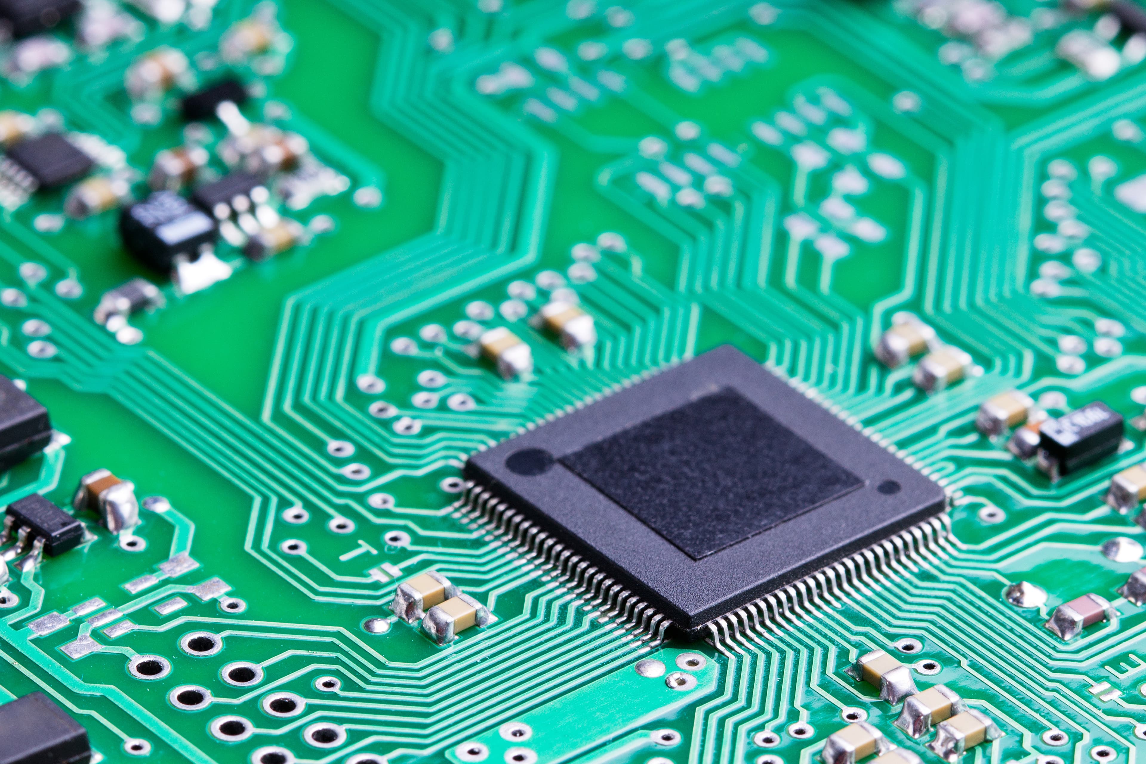
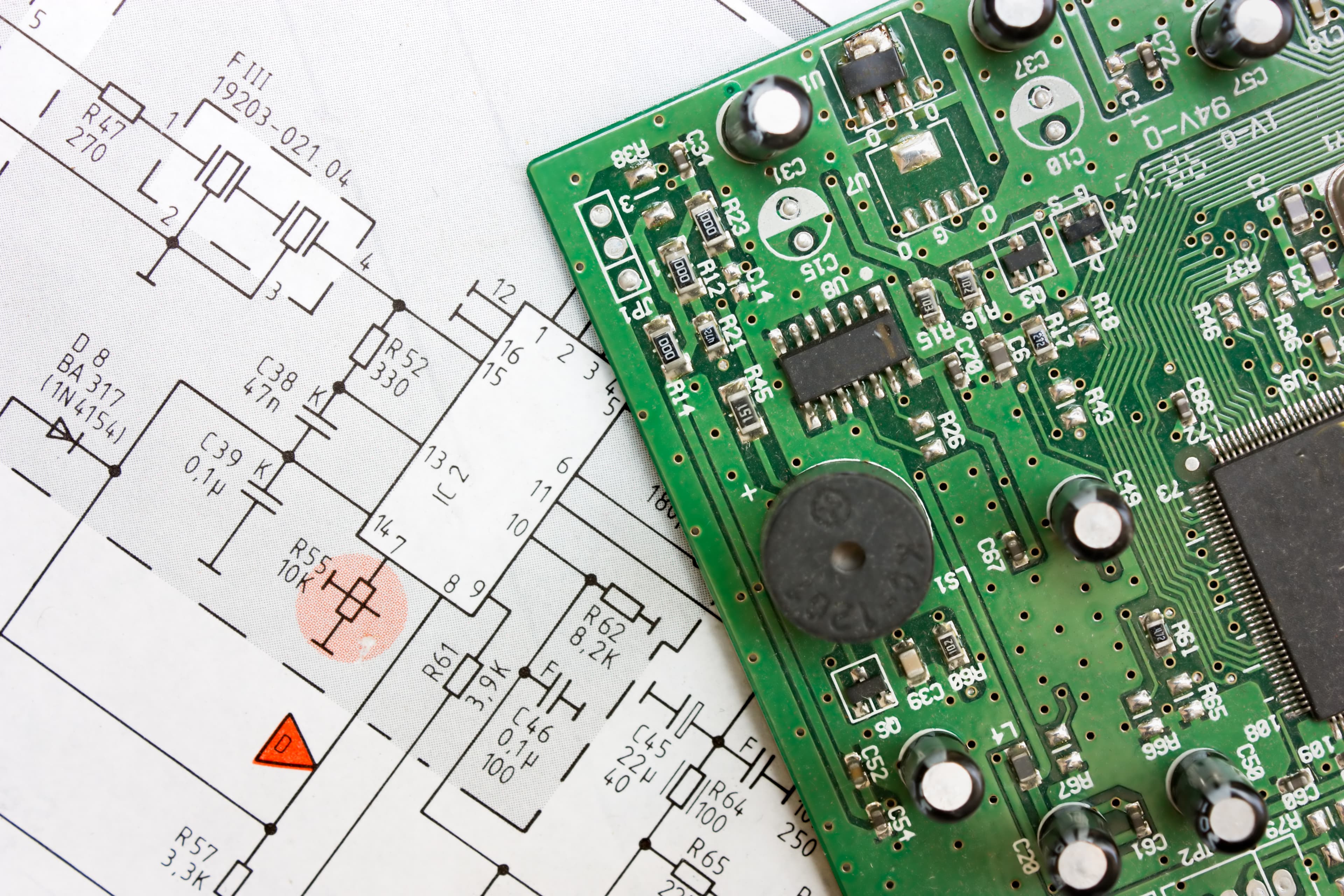
When someone places an order for a silkscreened printed circuit board, we know they understand how important silkscreening i. Silkscreen is made up of a layer of ink traces. These ink traces are used to help identify components, parts of a PCB, and test points. In addition to this, they also help to identify logos, marks, and symbols.
The silkscreen is commonly applied to the component side. However, it’s also quite usual for silkscreen to be applied on the solder side. Unfortunately, it may mean that the price may rise due to the work involved. However, a PCB that has been silkscreened can help the engineer and the manufacturer to identify and locate all of the required components.
The ink that is used in the silkscreen process is non-conductive epoxy ink. It’s important that this ink is used as power needs to travel to the components rather than the silkscreen. The ink that is used to make the required markings is formulated and available in a range of colors. The typical colors that are used are yellow, black, and white.
What Is The Process And Methods?
There are different methods used when silkscreen printed circuit boards are produced. Each manufacturer may have a preference for a particular method. However, the more methods they use, the more they can offer their customers.
Silkscreen and its importance
Silkscreen is hugely important to printed circuit board manufacturing. These days, there are 3 silk screening techniques that are commonly used, these are:
Direct legend printing – This method is by far the most accurate. However, because of this, it is more expensive. The process involves an inkjet printer applying acrylic ink to the PCB straight from the CAD data. Cured with UV light while it is printed, this method does not work on PCBs that have a silver finish.
Liquid photo imaging – This method tends to be used when the lines have a width that is greater than 4 mil. Similar to the process that is used to apply solder mask, liquid photo imaging involves liquid photo-imageable epoxy being coated on the laminate. Once the epoxy is added, it will be exposed to UV light. Once this stage is over, the board will then be developed and cured. Liquid photo imaging tends to be a lot more accurate than manual screening.
Manual screen printing – When the registration tolerance is 0.005 inches or the line widths are more than 0.007 inches, manual screen printing may be used. This procedure is undertaken using a stencil that is comprised of the text and traces. Every single trace is made using nylon. During the manufacturing process, the ink is directed through a stencil. This stencil is located on the laminate or layer. Once the ink has been added, it is cured in an oven. While manual screen printing is an easy way to create a silkscreen layer, learning how to use this method can take a lot of time.
Silkscreen Process
The silkscreen process is known as one of the sub-process of printed circuit board manufacturing. However, it is one of the most sophisticated processes. In fact, the silkscreen process has 32 different steps, which can be put into 6 processing areas:
1 – PCB silkscreen design
At this stage, your design will be printed onto the PCB. Computer-aided design (CAD) software is used here. The design will play an integral part in the PCB-manufacturing process. Only when the design is right will the PCB work well. This is why we always take a close look at any design you send us. We want your PCB to work well the first time it is used.
2 – Preparation of the board
As soon as the CAD blueprint has been finalized, it will be time to prepare the board. This step involves selecting the type of board that is required. As soon as the right material is selected, it will be cleaned, subjected to tape trolling, and board handling. Now the board will be ready for printing.
3 – Silkscreen printing
At this stage, the silkscreen will be printed on the printed circuit board. The board will be fixed to the machine and the screen itself will move so the ink can be added. The PCB that is etched will be aligned and the chosen ink colors will be added.
4 – Handling procedures
The correct handling mechanism is crucial so that the PCB’s quality is not affected. It also makes sure that the information that has been added to the PCB meets the required criteria. If we find any errors at this stage we will rectify them immediately. This is to ensure that you only ever receive high quality printed circuit boards.
5 – Inspection
During this stage, the PCB undergoes an inspection. This is to check the quality of the PCB panels. It is important at this stage that there are no misprints and no information is missing. If we find any issues during the inspection stage, we will take action immediately.
6 – Silkscreen treatment
Finally, the silkscreen undergoes treatment and another inspection. As soon as the PCB has passed our high standards, it can be sent to you. We want all of our customers to receive high-quality printed circuit boards each and every time. This is why we go further for you.
CONTACT US TODAY FOR A CONSULTATION
If you have any questions or queries about our silk screening pcb process, please talk to us. We are here to help you with all of your PCB-related needs. Alternatively, you may wish to contact us for a consultation. We will be happy to talk with you about your PCB silkscreen needs.
We have been in this industry for 40 years, and we know how to give our customers what they are looking for. Contact us today for a consultation at 602-866-7227. We look forward to hearing from you.