A Complete Guide To Home PCB Fabrication
Are you interested in home PCB fabrication? The process of creating your own printed circuit boards can be quite enjoyable. Please note, the creation process can be difficult, but it can also be rewarding. Being able to create your own printed circuit boards means you can potentially get many different devices to work.
Contact us today for a PCB fabrication quote. You can call us at 602-866-7227. We’re here to help you with all of your printed circuit board needs.
Can You Fabricate PCB’s At Home?
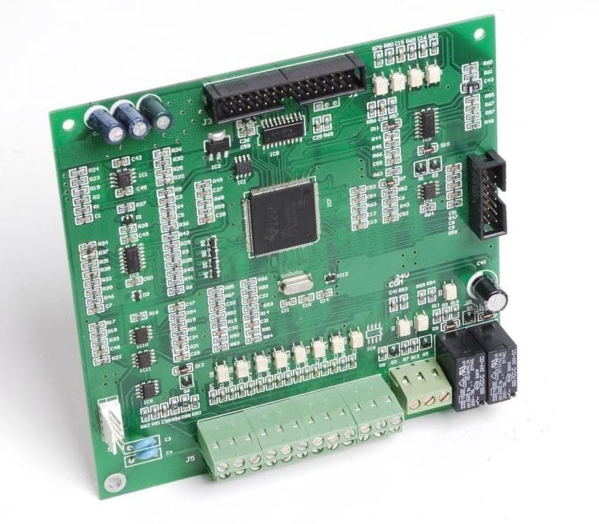
If you are a lover of all things electronic, you will no doubt have seen quite a lot of printed circuit boards around. Boards such as these help to make all of our lives easier. They do this by getting rid of the need for many breadboards and connecting wires. In addition to this, if the printed circuit boards you see are designed well, they can reduce the size of the device you’re using.
It is entirely possible for you to create a range of devices at home and from scratch. Sometimes there is nothing more satisfying than fabricating a PCB and creating a device. This is something that you could potentially do.
A printed circuit board works to support and connect electrical components. It does this by using conductive tracks, and other components. Many of these components and some features are etched from copper sheets. They are then laminated onto what is known as a “non-conductive substrate”.
On every printed circuit board you can find pre-designed copper tracks located on a conducting sheet. These tracks help to reduce the amount of wiring that is needed. This results in there being fewer faults. Many faults can arise due to the presence of loose connections. This is one of the great things about printed circuit boards, they can help to make the creation process a more satisfying and effective one.
Printing The PCB Layout
Printing the PCB layout is easier than you think. You don’t need much equipment to be able to do this. You will need to have a laser printer and some A4 glossy paper or photo paper. You will also need to:
- Remove the mirror print
- Make sure that the output is in black on the PCB software settings and your printer driver settings
- Ensure that the printout is always made on the paper’s glossy side
If you can, make two circuit boards that are exactly the same. This will ensure that you have a spare should you make a mistake.
Getting The Board Ready For Transfer
The next thing you need to do is to cut the copper plate so you can create the circuit board. Use a cutter or a hacksaw to cut the copper board to the correct size. Measure twice and cut once. As soon as you have cut the copper plate, you will need to rub the copper side of the board. Do this using either some abrasive sponge scrubs or some steel wool.
When you rub the copper side of the board you will remove the top oxide layer in addition to the photoresist layer. This is what you want as it will make using the PCB so much more effective. Once you have removed this layer it will be time to sand the surfaces. This will ensure that the image from your glossy or photo paper can stick better. If the image does not stick well it will mean you’re less able to place the components exactly where they need to be. This could potentially result in your printed circuit board failing to work as well as it should, if at all.
Transferring The Printout To The PCB
The next step in the printed circuit board creation process involves getting the pcb ready for transfer. There are two different methods that you could use for this process:
IRON ON THE GLOSSY PAPER
Once you have printed out the PCB image on your laser printer you will need to transfer it to the board. Be sure to flip the top layer horizontally. Palace the board’s copper surface on the printout. Make sure that the board is correctly aligned. It needs to be aligned with the PCB layout’s borders. Use some tape to hold both the printed paper and the board in the right position.
DRAW BY HAND ON THE PCB
If your circuit is relatively small and simple, you can draw the circuit by hand. Be sure to draw a basic sketch onto the copper plate. Do this using a pencil. As soon as your sketch looks good enough, trace over it. Use a permanent marker, preferably a black one. You’re a lot less likely to scuff or accidentally erase a permanent marker, so make sure you always use one at this stage.
Double check that the circuit is correct so that you can begin the next stage.
The next step in the PCB creation process involves ironing the circuit from the glossy or photo paper and onto your PCB plate.
Once you have printed the layout you will need to iron it making sure the image side is facing down. Next, heat up your iron to its highest temperature. Once you have done this, place the board and the photo paper on a clean table (preferably a wooden table that’s covered with a tablecloth). Ensure that the back of the photo paper is facing you.
Take a spatula or some pliers and hold one end of the board, ensuring that it is steady. Now place the iron on the opposite end for up to 10 seconds. Iron the photo paper, using the tip of the iron. Apply constant pressure for up to 15 minutes. Pay particular attention to the board’s edges. You will need to iron slowly while constantly applying pressure. Try to achieve a long, hard press as it works better than constantly moving the iron over the board.
The heat from your iron will transfer the ink from your photo or glossy paper to your copper plate. Try to avoid touching the copper plate as it will be hot.
Once you have finished ironing the board, plate it in some lukewarm water for approximately 10 minutes. This will help the paper to dissolve and make it so much easier to remove. When it comes to removing the paper, remove it from a low angle if you can.
You may find that some of the tracks look faint once you have removed the paper. Use a permanent marker to carefully make the tracks darker. Once you have done this, you’re ready to move on to the next step.
Etching The Board
This step needs to be carried out carefully. There is always the potential for you to make a mistake which could mean you’ll need to begin the process again.
Here’s what you need to do:
- Put on some plastic or rubber gloves
- Place some newspaper on the floor beneath where you are working. This is to ensure that your etching solution is less likely to damage it. You may also want to place some newspaper on the desk or table that you’re working on.
- Fill up a plastic box with water. Ensure that the plastic box doesn’t leak and is big enough to hold your circuit board. Ideally, your box should hold at least half a liter of fluid.
- Take some ferric chloride powder and dissolve 2-3 teaspoons of it in the water. Stir it, making sure that the powder dissolves. Try not to get any of the solution on your hands as it can turn your hands orange.
- Dip your printed circuit board into the solution for around 30 minutes. The length of time ensures that the ferric chloride solution (FeC13) reacts with any unmasked copper it comes across. It also works to remove the unwanted copper from the board in a process known as “Etching”.
- Once the 30 minutes is up, use some pliers and take your PCB out of the solution. Check to see if the unmasked copper has been etched. If it has not, place your PCB back into the solution for a little longer.
- As soon as all of the unmasked copper has been etched, you will need to dispose of the solution. Make sure that you dispose of it safely. The solution is poisonous to water-based organisms and fish. This is why you should not pour the solution down your sink. The solution could also damage your pipes. You, therefore, need to find an alternative method of disposal.
The next step in the printed circuit board creation process involves cleaning your PCB. Take some nail polish remover or thinner and place a small amount on some cotton wool. Carefully wipe your PCB so that the ink/toner on the plate is removed. The copper surface will then be exposed. Rinse the PCB carefully and dry it with some kitchen paper or a clean cloth. Finally, trim your new PCB to the correct size, and smoothen its edges with some sandpaper.
PCB Assembly
When it comes to assembling your printed circuit board, it makes sense to have all of the tools you need before you make a start.
You will need to have:
- Your printed circuit board(s)
- Stencil and syringe
- Solder paste and scraper
- Solder wire, tweezers, iron
As soon as you have all of the above items, you are ready to begin assembly.
The first thing that you need to do is to apply the solder paste to the printed circuit board. You can use a solder paste stencil should you wish to. Stencils such as these can ensure you have a repeatable solder paste application. In addition to this, they also make applying the solder very easy.
Take a syringe and place a very small amount of solder paste onto each of the pads on your PCB.
POPULATING THE PRINTED CIRCUIT BOARD
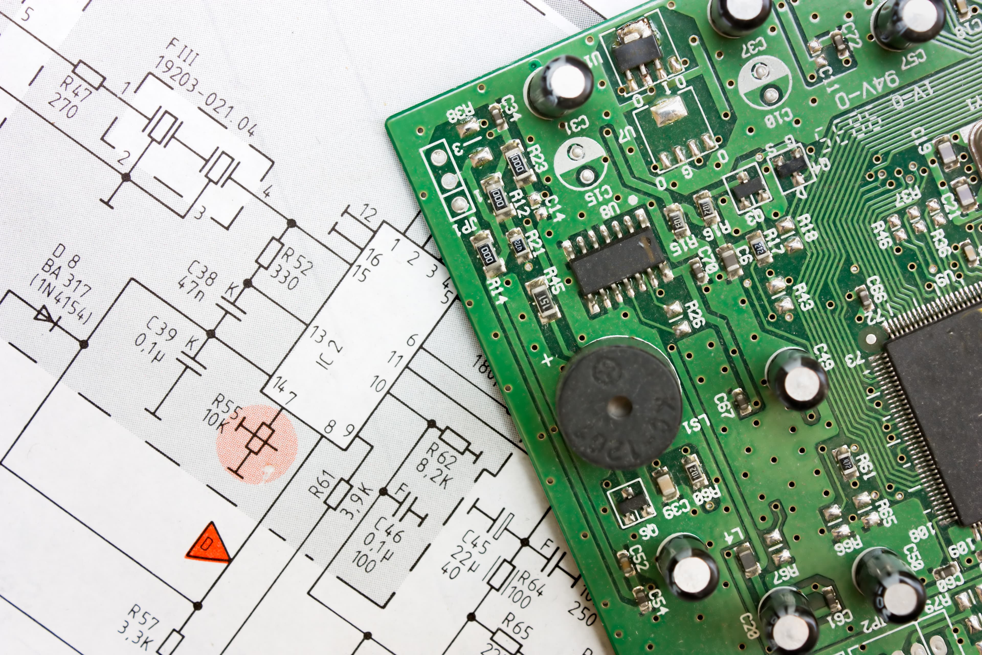
As soon as you have applied the solder paste, you need to place the components on your board using your tweezers. Having a diagram of your PCB will help you to identify where each of the components goes.
Place all of the components carefully and ensure that they are coupled on the back of your board. You should do this once they are correctly oriented.
Now your components are in place, you need to reflow your PCB. This involves heating your board until the solder paste is melted. As soon as your board cools, you will find that some permanent solder joints have been made. These joints will have been made between the pads and components on your PCB.
You can reflow your PCB using a reflow oven, hotplate, reflow skillet, or even a modified toaster oven. As soon as you have undertaken the reflowing process, you will need to examine your PCB. Take a good look at each of the components on your board. Make sure that none of your pads has moved. You also need to be on the lookout for solder bridges. These bridges can create short circuits.
– Temperature
The correct temperature will make sure that the soldering joints are high quality. Using an optimized reflow profile is essential here. The temperature of your reflow profile should ideally be no higher than 410°F if your board’s temperature is 284°F.
– Soldering
Now it’s time for you to solder the components onto your board. You will need to have an iron, solder wire, and flux to do this. Please note, your components should be ready to go. You should ideally wear antistatic gloves when you’re soldering. Also, make sure that you don’t touch the PCB pad directly. Try to keep the solder between the 200°F to 300°F range. Solder that is too cold will not work well. If the solder is too hot, it could damage the components.
As soon as you have added your components, you need to do a function test to make sure that every component works well. If you find a fault, be sure to deal with it as soon as you can. The sooner you do, the less likely it is to cause problems when using your printed circuit board.
You may need to remove some of the solder and re-attach a component. Just make sure that no solder bridges have formed as they can create a short circuit.
CALL US TODAY FOR A PCB FABRICATION QUOTE
If the idea of home PCB fabrication is something that appeals to you, we can help. We can supply components to you, or simply help you with some stages of fabrication. It doesn’t matter whether you create PCBs at home, in your garage, or in your factory, we can help you with all of your printed circuit board needs. We’re a friendly, experienced team that is here for you.
Alternatively, if you think the printed circuit board creation process is too complicated, again, we can help you. Here at Avanti circuits, we have been working in the PCB industry for almost 40 years. We are more than happy to answer your questions, especially if you would like us to make some printed circuit boards for you.
Contact us today for a PCB fabrication quote. You can call us at 602-866-7227.